Showing posts with label to. Show all posts
Showing posts with label to. Show all posts
Saturday, April 13, 2013
Voltage to current converter with floating load
The current in the feedback loop depends on the voltage and Ri.
This applications where we need to pass a constant current through a
load and hold it constant despite any changes in load resistance or load
voltage. When the load does not have to be grounded, we simply place
the load in the feedback loop and control both input and load current from this circuit.
This applications where we need to pass a constant current through a
load and hold it constant despite any changes in load resistance or load
voltage. When the load does not have to be grounded, we simply place
the load in the feedback loop and control both input and load current from this circuit.

This circuit shown in figure voltage to current converter
with floating load. The voltage to current converter can be used in
such applications as low voltage dc and a voltmeters, diode match
finders light emitting diodes (LEDS) and zener diode tester.
with floating load. The voltage to current converter can be used in
such applications as low voltage dc and a voltmeters, diode match
finders light emitting diodes (LEDS) and zener diode tester.
This circuit diagram Figure shows a voltage to current converter in which load resistor RL is
floating (not connected to ground). The input voltage is applied to the
no inverting input terminal and the feedback voltage cross R1 drives the inverting input terminal. This circuit is also called a current series negative feedback amplifier because the feedback voltage across R1 (applied to the inverting terminal) depends on the output current i0 and is in series with the input difference voltage vid.
floating (not connected to ground). The input voltage is applied to the
no inverting input terminal and the feedback voltage cross R1 drives the inverting input terminal. This circuit is also called a current series negative feedback amplifier because the feedback voltage across R1 (applied to the inverting terminal) depends on the output current i0 and is in series with the input difference voltage vid.

Friday, April 12, 2013
Simple Pulse train to sinusoid converter
The circuit letsyou convert a serial pulse stream or sinusoidal input to a sinusoidal output at 1/32 the frequency. By varying the frequency of Vrn, you can achieve an output range ofl07:1-from about 100 kH2 to less than 0.01 H2. The output resembles that of a 5-bit d/a converter operating on paralleLdigital data. Counter IC1 generates binary codes that repeatedly scan the range from 00000 to 11111. The output amplifier adds the corresponding XOR gate outputs, Vvv or ground, weighted by the values of input resistors R1 through R4.

The 16 counter codes 00000 to 01111, for instance, pass unchanged to the XOR gate outputs, and cause Vom to step through the half-sinusoidal cycle for maximum amplitude to minimum amplitude. Counter output Q4 becomes high for the next 16 codes, causing the XOR gates to invert the QO through Q3 outputs. As a result, VouT steps through the remaining half cycle from minimum to maximum amplitude. The counter then rolls over and initiates the next cycle. You can change the R1 through R4 values to obtain other VouT waveforms. VDv should be at least 12 V to assure maximum-frequency operation from IC1 to IC2.
Monday, April 8, 2013
How to Make a Small Homemade Automatic Voltage Stabilizer for TV sets and Refrigerator
A voltage stabilizer is a device which is used to sense inappropriate voltage levels and correct them to produce a reasonably stable output at the output where the load is connected.
Referring to the figure we find that the whole circuit is configured with the single op amp IC 741. It becomes the control section of the whole design.
Here we will study the design of a simple automatic mains AC voltage stabilizer which can be applied for the above purpose.
How the Circuit Functions
Referring to the figure we find that the whole circuit is configured with the single op amp IC 741. It becomes the control section of the whole design.
The IC is wired as a comparator, we all know how well this mode suits the IC 741 and other op amps. Its two inputs are suitable rigged for the said operations.
Sunday, April 7, 2013
8 to 18 volts TDA2005 Power Amplifier
This time, there is a series of audio amplifer 20W as well, but using IC TDA 2005 as a series of his base amplifier. The series of 2x20 Watt Audio Power Amplifier using TDA2005 can you see in the picture below.

Technical Data:
Performance of TDA2005M: (for this circuit); At 4.14 V supply voltage: 2 x 20 watts (stereo) into 4 Ohms.
Distortion: Approx. 0.2% at 4 Watts into 4 ohm load.Frequency Range: Approx. 20 Hz to 22 KHz.
Input Sensitivity: Approx. maximum 150 mV rms. .
Power supply: + 8 to 18 volts, approx. 3.5 Amps maximum per channel.
source [link]
Saturday, April 6, 2013
Build a LT3582 12 DC 5V to 12V DC Converter
Using LT3582-12 dual channel DC DC converter integrated circuit, manufactured by Linear Technology, can be designed a very simple step up dc converter. This 5 to 12V c converter electronic project provide both positive and negative outputs required in many biasing applications such as active matrix OLED (organic light-emitting diode)displays as well as CCD (charge coupled device) applications.

The LT3582 offer an I2C interface that can dynamically program output voltages, power sequencing and output voltage ramps as the application requires. The LT3582’s positive output voltage can be set between 3.2V and 12.775 in 25mV steps, whereas the negative output can be set between -1.2V and -13.95V in 50mV steps. The LT3582-12 is preconfigured with ±12V output, requiring no future programming.
Friday, April 5, 2013
6 to 12 Volt Power Supply Inverter
This inverter circuit can provide up to 800mA of 12V power from a 6V supply. For example, you could run 12V car accessories in a 6V (British?) car. The circuit is simple, about 75% efficient and quite useful. By changing just a few components, you can also modify it for different voltages.
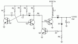
Part List:
R1, R4 2.2K 1/4W Resistor
R2, R3 4.7K 1/4W Resistor
R5 1K 1/4W Resistor
R6 1.5K 1/4W Resistor
R7 33K 1/4W Resistor
R8 10K 1/4W Resistor
C1,C2 0.1uF Ceramic Disc Capacitor
C3 470uF 25V Electrolytic Capcitor
D1 1N914 Diode
D2 1N4004 Diode
D3 12V 400mW Zener Diode
Q1, Q2, Q4 BC547 NPN Transistor
Q3 BD679 NPN Transistor
L1 See Notes
MISC Heatsink For Q3, Binding Posts (For Input/Output), Wire, Board
ReadMore....
Part List:
R1, R4 2.2K 1/4W Resistor
R2, R3 4.7K 1/4W Resistor
R5 1K 1/4W Resistor
R6 1.5K 1/4W Resistor
R7 33K 1/4W Resistor
R8 10K 1/4W Resistor
C1,C2 0.1uF Ceramic Disc Capacitor
C3 470uF 25V Electrolytic Capcitor
D1 1N914 Diode
D2 1N4004 Diode
D3 12V 400mW Zener Diode
Q1, Q2, Q4 BC547 NPN Transistor
Q3 BD679 NPN Transistor
L1 See Notes
MISC Heatsink For Q3, Binding Posts (For Input/Output), Wire, Board
source:LINK
How to Drive a Relay through an Opto Coupler Circuit
The following post describes how to drive a relay by using an isolated method, or through an opto coupler device.
The question was asked by one of the interested members of this blog, Miss Vineetha.
Before studying the proposed design, lets first understand how an opto coupler works.
An opto-coupler is a device which encapsules an LED and a photo-transistor inside a hermetically sealed, water proof, light proof package in the form of an 8 pin IC (resembling a 555 IC).
The LED is terminated over a couple of pin outs, while the three terminals of the photo-transistor is terminated over the other three assigned pin outs.
The idea is simple, its all about providing an input DC from the source which needs to be isolated to the LED pin outs via a limiting resistor (as we normally do with usual LEDs) and to switch the photo transistor in response to the applied input triggers.
The above action illuminates the internal LED whose light is detected by the photo-transistor causing it to conduct across its relevant pin outs.
The photo-transistor output is normally used for driving the preceding isolated stage, for example a relay driver stage.
As shown in the following circuit diagram, the relay driver may consist a NPN transistor or a PNP transistor.
If its a PNP transistor, the base is coupled at the collector of the photo transistor, alternatively, if a NPN transistor is used in the relay driver, the trigger is received from the emitter of the photo transistor quite like a Darlington paired configuration.
The rest of the operations are self evident.

The question was asked by one of the interested members of this blog, Miss Vineetha.
Before studying the proposed design, lets first understand how an opto coupler works.
An opto-coupler is a device which encapsules an LED and a photo-transistor inside a hermetically sealed, water proof, light proof package in the form of an 8 pin IC (resembling a 555 IC).
The LED is terminated over a couple of pin outs, while the three terminals of the photo-transistor is terminated over the other three assigned pin outs.
The idea is simple, its all about providing an input DC from the source which needs to be isolated to the LED pin outs via a limiting resistor (as we normally do with usual LEDs) and to switch the photo transistor in response to the applied input triggers.
The above action illuminates the internal LED whose light is detected by the photo-transistor causing it to conduct across its relevant pin outs.
The photo-transistor output is normally used for driving the preceding isolated stage, for example a relay driver stage.
As shown in the following circuit diagram, the relay driver may consist a NPN transistor or a PNP transistor.
If its a PNP transistor, the base is coupled at the collector of the photo transistor, alternatively, if a NPN transistor is used in the relay driver, the trigger is received from the emitter of the photo transistor quite like a Darlington paired configuration.
The rest of the operations are self evident.
Thursday, April 4, 2013
How to Make a Long Duration Timer Circuit
A timer in electronics is essentially a device which is used for producing time delay intervals for switching a connected load. The time delay is set externally by the user as per the requirement.
A simple timer can be built through many countless options. You can transistors, CMOS gates like NAND gates, NOT gates, linear ICs like 555, 741, 324, or simply more specific type of CMOS IC like the 4060.
All these devices besically generate oscillations which are adjustable right from a few Hz a second to a atomic fraction of a Hz.
Further more these ICs can be integrated together to form more complex timer circuits that may be used for generating very long time intervals.
In this post we see how two different modes of ICs are coupled together to form a long duration timer circuit.
Referring to the circuit diagram.
IC1 is an oscillator counter IC consisting a built in oscillator stage and generates clock pulses with varying periods across its pins 1,2,3,4,5,6,7,9,13,14,15.
The output from pin 3 produces the longest time interval and therefore we select this output for feeding the next stage.
The pot P1 and the capacitor C1 of IC1 can be used for adjusting the time span at it pin 3.
The higher the setting of the above components the longer the period at pin #3.
The next stage consists of decade counter IC 4017 which does nothing but increase the time interval obtained from IC1 to ten folds. It means if the the time interval generated by IC1s pin #3 is 10 hours, the time generated at pin #11 of IC2 would be 10*10 = 100 hours. Similarly if the time generated at pin #3 of IC1 is 6 minutes, would mean a high output from pin#11 of IC1 after 60 minutes or 1 hour.
When power is switched ON, capacitor C2 makes sure that the reset pins of both the ICs are appropriately reset, so that the ICs begin counting from zero rather than from some irrelevant intermediate figure.
As long as the counting progresses, pin #11 of IC2 remains at logic low, such that the relay driver is held switched OFF.
After the set timing lapses, pin#11 of IC2 goes high activating the transistor/relay stage and the subsequent load connected with the relay contacts.
The diode D1 ensures that the output from pin#11 of IC2 locks the counting of IC1 by providing a feed back latch signal at its pin #11.
Thus the whole timer latches until the timer is switched OFF and restarted again for repeating the entire process.
 Parts List
R1, R3 = 1M
R2, R4 = 1K,
C1, C2 = 1uF/25V,
D1, D2 = 1N4007,
IC1 = 4060,
IC2 = 4017,
T1 = BC547,
POT = 1M linear
RELAY = 12V SPDT
A simple timer can be built through many countless options. You can transistors, CMOS gates like NAND gates, NOT gates, linear ICs like 555, 741, 324, or simply more specific type of CMOS IC like the 4060.
All these devices besically generate oscillations which are adjustable right from a few Hz a second to a atomic fraction of a Hz.
Further more these ICs can be integrated together to form more complex timer circuits that may be used for generating very long time intervals.
In this post we see how two different modes of ICs are coupled together to form a long duration timer circuit.
Referring to the circuit diagram.
IC1 is an oscillator counter IC consisting a built in oscillator stage and generates clock pulses with varying periods across its pins 1,2,3,4,5,6,7,9,13,14,15.
The output from pin 3 produces the longest time interval and therefore we select this output for feeding the next stage.
The pot P1 and the capacitor C1 of IC1 can be used for adjusting the time span at it pin 3.
The higher the setting of the above components the longer the period at pin #3.
The next stage consists of decade counter IC 4017 which does nothing but increase the time interval obtained from IC1 to ten folds. It means if the the time interval generated by IC1s pin #3 is 10 hours, the time generated at pin #11 of IC2 would be 10*10 = 100 hours. Similarly if the time generated at pin #3 of IC1 is 6 minutes, would mean a high output from pin#11 of IC1 after 60 minutes or 1 hour.
When power is switched ON, capacitor C2 makes sure that the reset pins of both the ICs are appropriately reset, so that the ICs begin counting from zero rather than from some irrelevant intermediate figure.
As long as the counting progresses, pin #11 of IC2 remains at logic low, such that the relay driver is held switched OFF.
After the set timing lapses, pin#11 of IC2 goes high activating the transistor/relay stage and the subsequent load connected with the relay contacts.
The diode D1 ensures that the output from pin#11 of IC2 locks the counting of IC1 by providing a feed back latch signal at its pin #11.
Thus the whole timer latches until the timer is switched OFF and restarted again for repeating the entire process.
R1, R3 = 1M
R2, R4 = 1K,
C1, C2 = 1uF/25V,
D1, D2 = 1N4007,
IC1 = 4060,
IC2 = 4017,
T1 = BC547,
POT = 1M linear
RELAY = 12V SPDT
Subscribe to:
Posts (Atom)